
Table of Contents
Sequence 1: The Original
Design
Sequence 2: Simple
Alternating Sequence
Sequence 5: Double
Zig-Zag Sequence
Sequence 7: Reverse Spin
Sequence
Frequency Divider VHDL
Listing
Sequence 1: Original
Design Sequence
Sequence 2: Simple
Alternating Sequence
Sequence 5: Double Zig
Zag Sequence
Sequence 7: Reverse Spin
Sequence
Top-Level Component VHDL
Listing
Introduction
This Christmas Light decoration is a project I conceived many years ago with the idea of having each of the letters that make up the words Merry Christmas light up on its own. The idea originated back when I was in middle school and was based on a simpler project I was working on at the time. This project was built with a small cardboard box, a light that was capable of blinking on and off, and a DC power source. To describe it as simply as possible, this project was built up by drawing the letters of Merry Christmas on one side of the box, then taking a piece of a red plastic bag and lining it across the inside of the side with the letters cut out. Aluminum foil was used to line the remaining sides to reflect the light from the light bulb to make the letters brighter. The light bulb was then wired to a DC power source and placed inside the box. The bulb itself was one of those flashing bulbs that came from a string of lights that go to a Christmas tree, therefore I manage to get the effects of a flashing light using the most basic DC source to light bulb circuit with a switch in between.
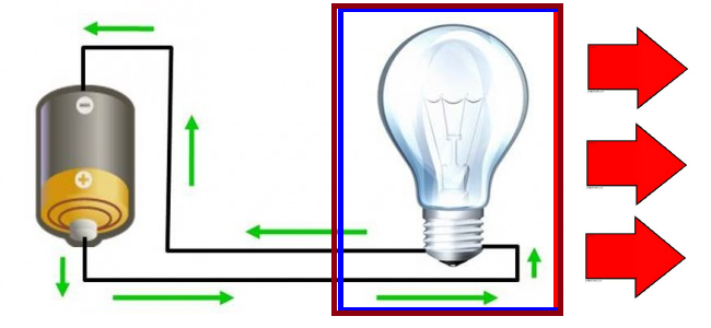
Figure 1:
Christmas Light Decoration Middle School Diagram
The red arrows indicate desired light direction.
The brown box had the letters Merry Christmas cut into the side lined with red
plastic.
This simple project was a marvel to those who observed it functioning at the time and gave me some ideas on how I could make it even more dazzling. I had envisioned separating the letters and lighting them up individually, perhaps in a pattern or some sort. However, at the time, my knowledge of electronics was limited on experiments I did at home and what I learned in my 4th grade science class. I did not know much about the various electronic components and their functions therefore, the idea was put aside for the time being.
Fast forward to my college years and after taking a digital electronics undergrad course I decided to design the Christmas light project that I had envisioned back in middle school. I knew from taking the course that I could achieve the pattern using a binary counter and decoder logic. After considering various circuits for generating the lights beginning with using small incandescent lights, I finally settled on using high brightness LEDs due to their much longer life expectancy and their smaller power requirements. At first I was going to simply implement red LEDs that turn on and off but later decided to include green LEDs that turn on when the red LEDs were off. After some consideration on how I could achieve this I concluded that this could be achieved by simply treating them as logic probes that operate like the off the shelf logic probe devices purchased at electronics stores. The original design consisted of a timer, a binary counter, and a set of gates that provided the decoder logic for one sequence. Given the more powerful capabilities of the Xilinx FPGA device and the use of VHDL to program it, I took this design a step further and added multiple sequences and multiple frequencies for the set of lights. The final design will be covered in greater detail in the following sections.
Christmas Light Decoration
The Christmas Light decoration project consists of 14 LEDs wired as logic probes with each probes lighting each of the letters in the words “Merry Christmas.” The heart of the design consists of a binary counter that continuously counts upwards from 0 to 15 with each rising edge of the clock signal. The outputs of the counter are then fed into the inputs of a decoder module that decodes the signals into one of eight selected patterns.
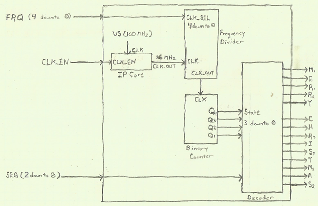
Figure 2: Christmas Light Decoration Block Diagram
This design was enhanced from the original design which consisted of a single 1 Hz frequency clock and a single sequence to provide a range of various frequencies and eight selectable sequences. The frequency is selected by 5 input switches for the FRQ input and 3 input switches for the SEQ input. From the block diagram, the design consists of a frequency generator, frequency divider, binary counter, and four-bit decoder that turns on and off the lights based on the output of the binary counter.
Frequency Generator
The frequency generator for this design comes from the 100 MHz oscillator clock provided by the Basys 3 trainer board used to develop and test this design. This clock is connected to pin W5 which is an MRCC input on bank 34 of the Artix-7 FPGA device.[1] The Clocking Wizard IP provided by the Xilinx Vivado tools is used by this design to generate a 16 MHz clock frequency used to drive the frequency divider component of this design.
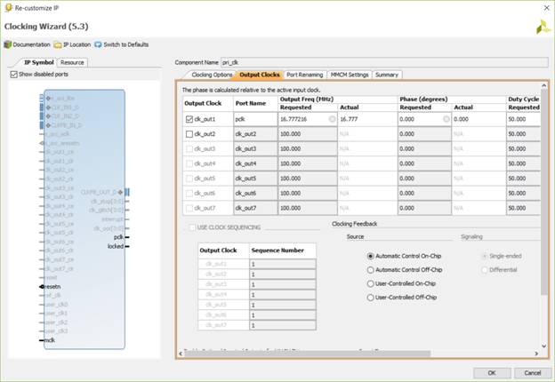
Figure 3: Xilinx Vivado Clocking Wizard IP
This Clock Wizard IP was customized to provide a 16 MHz output on the signal PCLK (primary clock) with the 100 MHz signal driving the MCLK (master clock) input. This wizard was also customized to provide an active low reset input (resetn) that will be driven by the master reset input from the top-level design.
Frequency Divider Stage
The primary clock output signal (PCLK) of the Clocking Wizard IP drives the clock input (CLK_IN) of the frequency divider stage. This stage takes the selected frequency provided by the five input switches (CLK_SEL) and divides the input frequency to provide a frequency output from 1 Hz to 16 Hz. The stage is designed to work optimally when only one of the 5 inputs are active and the output clock frequency is undefined if multiple inputs are active. I envisioned using a five-way rotary or sliding switch that activates only one of these inputs at a time for a final prototype. However, for the demonstration on the Basys 3 trainer board, five of the 16 available switches provided will be used.
This component consists of two processes written in
VHDL. The first process is a MHz to Hz
frequency divider that takes the 16 MHz signal and divides it to a 16 Hz signal
that is used by the second process. To
simplify this component, I attempted to make the output frequency of the
Clocking Wizard IP signal (used in the frequency generator stage) to be
16,777,216 Hz. Since this is 16 times
the value of 220, I could simply use the value of the 20th
bit of a 20-bit counter to generate the output signal of 16 Hz. The actual frequency output (as indicated by the
Clocking Wizard IP) of 16.777 MHz is “good enough for government use.”
|
-- The MHz to Hz stage of the frequency divider. MHz2Hz: process(CLK_IN) variable
mhertz_count : std_logic_vector(19 downto 0); begin -- Increment the count on the rising edge of the clock. if CLK_IN'event and CLK_IN = '1' then mhertz_count := mhertz_count + 1; end if; -- Set the clock in Hz signal to MSB of count. CLK_HZ <= mhertz_count(19); end process; |
|
VHDL
Listing for the MHz to Hz frequency divider process. |
The second process of the frequency divider component divides the 16 Hz output
signal of the previous process to a selectable set of output frequencies of 1,
2, 4, 8, or 16 Hz. This process works
optimally when only one of the selection inputs are active.
|
-- The frequency divider output stage. FRQDIV: process(CLK_HZ, CLK_SEL) variable count : std_logic_vector(4 downto 0); variable outp : std_logic_vector(4 downto 0); begin -- Increment count on rising edge of CLK_HZ. if CLK_HZ'event and CLK_HZ = '1' then count := count + 1; -- Setup the output clock port. for i in 4 downto 0 loop outp(i) := (CLK_SEL(i) and count(i)); end loop; end if; -- Set the output clock signal. CLK_OUT <= outp(4) or outp(3) or outp(2) or outp(1) or outp(0); end process; |
|
VHDL Listing for the selectable frequency divider output process. |
The complete listing of the VHDL source code for this component of the design is provided in the appendix section of this report. This component did not simulate properly using either the Xilinx Vivado or the Active HDL software but the final VHDL was synthesized and tested in the Basys 3 device.
Figure 4: Frequency Generator and Divider Testing (video)
The switches on the far-left control the frequency and the fifth switch from the right is the master reset. The LED on the far-right is the oscillating output of the frequency divider.
Binary Counter Stage
The binary counter is modelled after the 74161 synchronous presettable binary counter in VHDL. In this design, it is configured to count upwards continuously from 0 to 15 with none of the other functionality of the component being utilized. The output signals are connected to the decoder stage to decode the current count into one of the eight selectable light sequences. The functions of this device were derived in VHDL to mimic the following features and provide the following interface.[2]
|
Pin |
Symbol |
Description |
|
1 |
MR |
asynchronous master
reset (active low) |
|
2 |
CP |
clock input
(low-to-high, edge-triggered) |
|
3 |
P0 |
Parallel data input |
|
4 |
P1 |
Parallel data input |
|
5 |
P2 |
Parallel data input |
|
6 |
P3 |
Parallel data input |
|
7 |
CEP |
count enable input |
|
8 |
GND |
ground |
|
9 |
PE |
parallel load enable
input (active low) |
|
10 |
CET |
count enable carry
output |
|
11 |
Q3 |
counter output |
|
12 |
Q2 |
counter output |
|
13 |
Q1 |
counter output |
|
14 |
Q0 |
counter output |
|
15 |
TC |
terminal count output |
|
16 |
Vcc |
supply voltage |
74161 Presettable Binary Counter with Asynchronous Reset
|
Function Table |
||||
|
SR |
PE |
CET |
CEP |
Action on the rising clock edge. |
|
0 |
X |
X |
X |
Reset (clear) Q goes to zero. |
|
1 |
0 |
X |
X |
Load (Pn --> Qn) |
|
1 |
1 |
1 |
1 |
Count (Increment) |
|
1 |
1 |
0 |
X |
No Change (Hold) |
|
1 |
1 |
X |
0 |
No Change (Hold) |
|
Source: Motorola Fast and LS TTL
Data |
||||
This stage was implemented and tested like the lab exercise in module 4 that implemented and tested the MC14510B Up/Down BCD Counter in VHDL. Unlike that counter, the 74161 binary counter does not have bidirectional counting capability but it does utilize a terminal count (TC) output that functions similarly to the carry output of the MC14510B device. Like the BCD device, this device can also be configured in stages to allow for larger count values with 4-bits per stage. This feature, however, was not tested since it was not required for the larger design but the component itself was tested and simulated thoroughly.
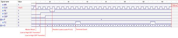
Figure 5: Simulation Results of the 74161 Binary Counter
The VHDL was also synthesized and tested using the Basys 3 device to ensure that there were no subtle differences between the simulation and how the component functions in actual hardware.
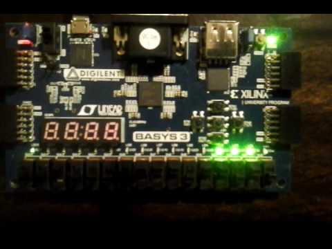
Figure 6: Testing Results of the Binary Counter (video)
The LEDs on the far right are the Q outputs of the binary counter and the switches just below them are the P inputs (set to 1010). During testing, the CET, CEP, and PE switches were tested to see their effects on the component. The LED on the far left is the TC terminal count output. The complete VHDL listing of the 74161 binary counter component is provided in the appendix.
The Decoder Stage
The decoder stage takes the outputs of the counter stage and decodes them according to the selected sequence. For each count of the binary counter (0 to 15) the decoder outputs a high or low voltage (1 or 0) for each of the letters of the words Merry Christmas per the truth table of the selected sequence. The design calls for 8 selectable sequences selected by the operator. The truth tables for each of the sequences show the patterns for the lights based on the outputs (A, B, C, and D signals) of the binary counter with a one for the letter indicating that the light will be red and a blank indicating the light will be green.
The decoding logic for each of the designs was accomplished by using Karnaugh Maps to determine the logic that drives each of the letters in the sequences. For brevity, the K-Maps will be provided in the appendix section along with the complete listing for this component. For each of the sequences the final decoder logic derived from each set of K-maps will be provided with the truth tables in the following subsections.
Sequence 1: The Original Design
This was the pattern I put together for an earlier design of this project that used TTL logic gates to decode the output of an actual 74161 binary counter. This pattern had to reduce well to limit the chip count for the final decoder circuit. Reducing the chip count for a circuit design ensures that the final design consume less power during operation and costs less to produce. Utilizing the 7400 series of components instead of programmable logic device enables me to build the design without requiring the use of expensive programmers.
|
A |
B |
C |
D |
M |
E |
R |
R |
Y |
C |
H |
R |
I |
S |
T |
M |
A |
S |
|
0 |
0 |
0 |
0 |
1 |
1 |
||||||||||||
|
0 |
0 |
0 |
1 |
1 |
1 |
1 |
1 |
1 |
1 |
||||||||
|
0 |
0 |
1 |
0 |
1 |
1 |
1 |
1 |
1 |
1 |
1 |
1 |
||||||
|
0 |
0 |
1 |
1 |
1 |
1 |
1 |
1 |
1 |
1 |
||||||||
|
0 |
1 |
0 |
0 |
1 |
1 |
||||||||||||
|
0 |
1 |
0 |
1 |
1 |
1 |
1 |
1 |
1 |
1 |
1 |
1 |
||||||
|
0 |
1 |
1 |
0 |
1 |
1 |
1 |
1 |
1 |
1 |
1 |
1 |
1 |
1 |
1 |
1 |
1 |
1 |
|
0 |
1 |
1 |
1 |
1 |
1 |
1 |
1 |
1 |
1 |
1 |
1 |
||||||
|
1 |
0 |
0 |
0 |
1 |
1 |
||||||||||||
|
1 |
0 |
0 |
1 |
1 |
1 |
1 |
1 |
1 |
1 |
||||||||
|
1 |
0 |
1 |
0 |
1 |
1 |
1 |
1 |
1 |
1 |
1 |
1 |
1 |
1 |
1 |
1 |
1 |
1 |
|
1 |
0 |
1 |
1 |
1 |
1 |
1 |
1 |
1 |
1 |
||||||||
|
1 |
1 |
0 |
0 |
1 |
1 |
||||||||||||
|
1 |
1 |
0 |
1 |
1 |
1 |
1 |
1 |
1 |
1 |
1 |
1 |
||||||
|
1 |
1 |
1 |
0 |
1 |
1 |
1 |
1 |
1 |
1 |
1 |
1 |
||||||
|
1 |
1 |
1 |
1 |
1 |
1 |
1 |
1 |
1 |
1 |
1 |
1 |
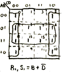
Truth Table for the Original Design Sequence
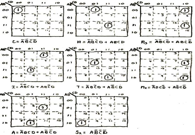
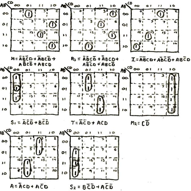
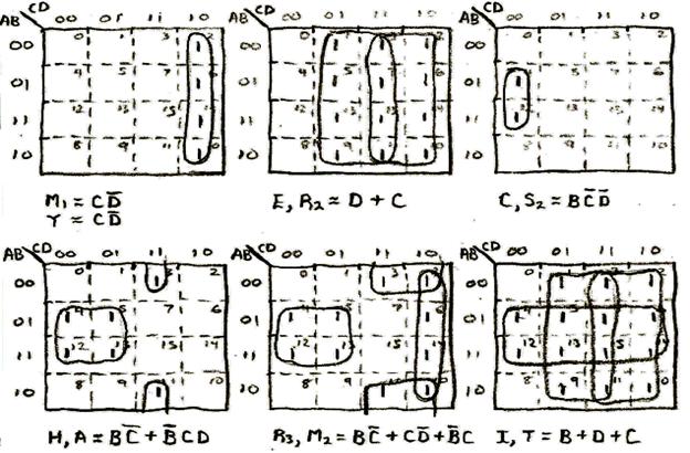
This sequence has a lot of symmetry and a lot of letters turning on at the same intervals within the sequence. Therefore, the final decoding reduces as follows:
M1, Y, C, H, A, S2 = C AND NOT(D);
E, R2, R3, I, T, M2 = D OR (NOT(A) AND B AND C) OR (A AND NOT(B) AND C);
R1, S1 = B OR NOT(D);
Sequence 2: Simple Alternating Sequence
This sequence just simply alternates between on and off for each letter as shown in the truth table.
|
A |
B |
C |
D |
M |
E |
R |
R |
Y |
C |
H |
R |
I |
S |
T |
M |
A |
S |
|
0 |
0 |
0 |
0 |
1 |
1 |
1 |
1 |
1 |
1 |
1 |
1 |
||||||
|
0 |
0 |
0 |
1 |
1 |
1 |
1 |
1 |
1 |
1 |
||||||||
|
0 |
0 |
1 |
0 |
1 |
1 |
1 |
1 |
1 |
1 |
1 |
1 |
||||||
|
0 |
0 |
1 |
1 |
1 |
1 |
1 |
1 |
1 |
1 |
||||||||
|
0 |
1 |
0 |
0 |
1 |
1 |
1 |
1 |
1 |
1 |
1 |
1 |
||||||
|
0 |
1 |
0 |
1 |
1 |
1 |
1 |
1 |
1 |
1 |
||||||||
|
0 |
1 |
1 |
0 |
1 |
1 |
1 |
1 |
1 |
1 |
1 |
1 |
||||||
|
0 |
1 |
1 |
1 |
1 |
1 |
1 |
1 |
1 |
1 |
||||||||
|
1 |
0 |
0 |
0 |
1 |
1 |
1 |
1 |
1 |
1 |
1 |
1 |
||||||
|
1 |
0 |
0 |
1 |
1 |
1 |
1 |
1 |
1 |
1 |
||||||||
|
1 |
0 |
1 |
0 |
1 |
1 |
1 |
1 |
1 |
1 |
1 |
1 |
||||||
|
1 |
0 |
1 |
1 |
1 |
1 |
1 |
1 |
1 |
1 |
||||||||
|
1 |
1 |
0 |
0 |
1 |
1 |
1 |
1 |
1 |
1 |
1 |
1 |
||||||
|
1 |
1 |
0 |
1 |
1 |
1 |
1 |
1 |
1 |
1 |
||||||||
|
1 |
1 |
1 |
0 |
1 |
1 |
1 |
1 |
1 |
1 |
1 |
1 |
||||||
|
1 |
1 |
1 |
1 |
1 |
1 |
1 |
1 |
1 |
1 |
Truth Table for the Simple Alternating Sequence
Due to the simplicity of this sequence, one only needs to look at the D output of the truth table to determine when the letters turn on or off for each interval. Letters M1, R1, Y, C, R2, S1, M2, and S2 are on when the D output is off and letters E, R2, H, I, T, and A are on when the D output is on.
M1, R1, Y, C, R3, S1, M2, S2 = NOT(D);
E, R2, H, I, T, A = D;
Sequence 3: Zig Zag Sequence
This sequence contains very little repeating patterns for the individual letters and no two letters followed the same pattern. Therefore, it was one of the most complicated to decode.
|
A |
B |
C |
D |
M |
E |
R |
R |
Y |
C |
H |
R |
I |
S |
T |
M |
A |
S |
|
0 |
0 |
0 |
0 |
1 |
1 |
||||||||||||
|
0 |
0 |
0 |
1 |
1 |
1 |
||||||||||||
|
0 |
0 |
1 |
0 |
1 |
1 |
||||||||||||
|
0 |
0 |
1 |
1 |
1 |
1 |
||||||||||||
|
0 |
1 |
0 |
0 |
1 |
1 |
||||||||||||
|
0 |
1 |
0 |
1 |
1 |
1 |
||||||||||||
|
0 |
1 |
1 |
0 |
1 |
1 |
||||||||||||
|
0 |
1 |
1 |
1 |
1 |
1 |
||||||||||||
|
1 |
0 |
0 |
0 |
1 |
1 |
||||||||||||
|
1 |
0 |
0 |
1 |
1 |
1 |
||||||||||||
|
1 |
0 |
1 |
0 |
1 |
1 |
||||||||||||
|
1 |
0 |
1 |
1 |
1 |
1 |
||||||||||||
|
1 |
1 |
0 |
0 |
1 |
1 |
||||||||||||
|
1 |
1 |
0 |
1 |
1 |
1 |
||||||||||||
|
1 |
1 |
1 |
0 |
1 |
1 |
||||||||||||
|
1 |
1 |
1 |
1 |
1 |
1 |
Truth Table for the Zig Zag Sequence
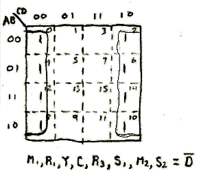
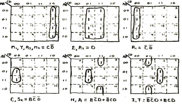
Due to no two letters having the same sequence, each of the letters had to be decoded individually.
M1 = NOT(B) AND NOT(C) AND NOT(D);
E = (NOT(B) AND NOT(C) AND D) OR (B AND C AND D);
R1 = C AND NOT(D);
R2 = (B AND NOT(C) AND D) OR (NOT(B) AND C AND D);
Y = B AND NOT(C) AND NOT(D);
C = NOT(A) AND NOT(B) AND NOT(C) AND NOT(D);
H = (NOT(A) AND NOT(B) AND NOT(C) AND D) OR (A AND B AND C AND D);
R3 = (NOT(A) AND NOT(B) AND C AND NOT(D)) OR (A AND B AND C AND NOT(D));
I = (NOT(A) AND NOT(B) AND C AND D) OR (A AND B AND NOT(C) AND D);
S1 = B AND NOT(C) AND NOT(D);
T = (NOT(A) AND B AND NOT(C) AND D) OR (A AND NOT(B) AND C AND D);
M2 = (NOT(A) AND B AND C AND NOT(D)) OR (A AND NOT(B) AND C AND NOT(D));
A = (NOT(A) AND B AND C AND D) OR (A AND NOT(B) AND NOT(C) AND D);
S2 = A AND NOT(B) AND NOT(C) AND NOT(D);
Sequence 4: Diamond Sequence
The diamond sequence expands and contracts the on states for the letters within the truth table to form a diamond pattern.
|
A |
B |
C |
D |
M |
E |
R |
R |
Y |
C |
H |
R |
I |
S |
T |
M |
A |
S |
|
0 |
0 |
0 |
0 |
1 |
1 |
||||||||||||
|
0 |
0 |
0 |
1 |
1 |
1 |
1 |
1 |
||||||||||
|
0 |
0 |
1 |
0 |
1 |
1 |
1 |
1 |
||||||||||
|
0 |
0 |
1 |
1 |
1 |
1 |
1 |
1 |
||||||||||
|
0 |
1 |
0 |
0 |
1 |
1 |
1 |
|||||||||||
|
0 |
1 |
0 |
1 |
1 |
1 |
1 |
1 |
||||||||||
|
0 |
1 |
1 |
0 |
1 |
1 |
1 |
1 |
||||||||||
|
0 |
1 |
1 |
1 |
1 |
1 |
1 |
1 |
||||||||||
|
1 |
0 |
0 |
0 |
1 |
1 |
||||||||||||
|
1 |
0 |
0 |
1 |
1 |
1 |
1 |
1 |
||||||||||
|
1 |
0 |
1 |
0 |
1 |
1 |
1 |
1 |
||||||||||
|
1 |
0 |
1 |
1 |
1 |
1 |
1 |
1 |
||||||||||
|
1 |
1 |
0 |
0 |
1 |
1 |
1 |
|||||||||||
|
1 |
1 |
0 |
1 |
1 |
1 |
1 |
1 |
||||||||||
|
1 |
1 |
1 |
0 |
1 |
1 |
1 |
1 |
||||||||||
|
1 |
1 |
1 |
1 |
1 |
1 |
1 |
1 |
Truth Table for the Diamond Sequence
The K-Maps decoded this table as follows:
M1, Y, R3, M2 = C AND NOT(D);
E, R2 = D;
R1 = NOT(C) AND NOT(D);
C, S2 = B AND NOT(C) AND NOT(D);
H, A = (B AND NOT(C) AND D) OR (NOT(B) AND C AND D);
I, T = (NOT(B) AND NOT(C) AND D) OR (B AND C AND D);
S1 = NOT(B) AND NOT(C) AND NOT(D);
Sequence 5: Double Zig-Zag Sequence
The double zig zag sequence takes two sets of lights and “zig zags” them side to side like the previous zig zag sequence pattern. Also, like the zig zag sequence in that there was little symmetry and no letters in the table that repeated the same pattern.
|
A |
B |
C |
D |
M |
E |
R |
R |
Y |
C |
H |
R |
I |
S |
T |
M |
A |
S |
|
0 |
0 |
0 |
0 |
1 |
1 |
1 |
1 |
||||||||||
|
0 |
0 |
0 |
1 |
1 |
1 |
1 |
1 |
||||||||||
|
0 |
0 |
1 |
0 |
1 |
1 |
1 |
1 |
||||||||||
|
0 |
0 |
1 |
1 |
1 |
1 |
1 |
1 |
||||||||||
|
0 |
1 |
0 |
0 |
1 |
1 |
1 |
1 |
||||||||||
|
0 |
1 |
0 |
1 |
1 |
1 |
1 |
1 |
||||||||||
|
0 |
1 |
1 |
0 |
1 |
1 |
1 |
1 |
||||||||||
|
0 |
1 |
1 |
1 |
1 |
1 |
1 |
1 |
||||||||||
|
1 |
0 |
0 |
0 |
1 |
1 |
1 |
1 |
||||||||||
|
1 |
0 |
0 |
1 |
1 |
1 |
1 |
1 |
||||||||||
|
1 |
0 |
1 |
0 |
1 |
1 |
1 |
1 |
||||||||||
|
1 |
0 |
1 |
1 |
1 |
1 |
1 |
1 |
||||||||||
|
1 |
1 |
0 |
0 |
1 |
1 |
1 |
1 |
||||||||||
|
1 |
1 |
0 |
1 |
1 |
1 |
1 |
1 |
||||||||||
|
1 |
1 |
1 |
0 |
1 |
1 |
1 |
1 |
||||||||||
|
1 |
1 |
1 |
1 |
1 |
1 |
1 |
1 |
Truth Table for the Double Zig Zag Sequence
Since none of the letters in the table repeated the same sequence, each letter had to be decoded individually.
M1 = (NOT(B) and NOT(C) and NOT(D)) or (B and NOT(C) and D) or (NOT(B) and C and D);
E = (B and NOT(C) and NOT(D)) or (NOT(B) and NOT(C) and D) or (B and C and D);
R1 = (NOT(B) and NOT(C) and NOT(D)) or (C and NOT(D));
R2 = D;
Y = (B and NOT(D)) or (C and NOT(D));
C = (NOT(A) and NOT(B) and NOT(C) and NOT(D)) or
(NOT(A) and B and NOT(C) and D) or
(A and NOT(B) and C and D);
H = (NOT(A) and NOT(B) and NOT(C) and D) or
(NOT(A) and B and C and NOT(D)) or
(A and NOT(B) and C and NOT(D)) or
(A and B and C and D);
R3 = (NOT(A) and NOT(B) and C and NOT(D)) or
(NOT(A) and B and C and D) or
(A and NOT(B) and NOT(C) and D) or
(A and B and C and NOT(D));
I = (NOT(A) and NOT(B) and C and D) or (A and NOT(B) and NOT(C) and NOT(D)) or
(A and B and NOT(C) and D);
S1 = (NOT(A) and NOT(C) and NOT(D)) or (B and NOT(C) and NOT(D));
T = (NOT(A) and NOT(C) and D) or (A and C and D);
M2 = C and NOT(D);
A = (NOT(A) and C and D) or (A and NOT(C) and D);
S2 = (B and NOT(C) and NOT(D)) or (A and NOT(C) and NOT(D));
Sequence 6: Spin Sequence
The spin sequence got its name due to the pattern in the table appearing as if there was a sort of spinning spiral going down the table.
|
A |
B |
C |
D |
M |
E |
R |
R |
Y |
C |
H |
R |
I |
S |
T |
M |
A |
S |
|
0 |
0 |
0 |
0 |
1 |
1 |
||||||||||||
|
0 |
0 |
0 |
1 |
1 |
1 |
1 |
1 |
||||||||||
|
0 |
0 |
1 |
0 |
1 |
1 |
1 |
1 |
1 |
1 |
||||||||
|
0 |
0 |
1 |
1 |
1 |
1 |
1 |
1 |
1 |
1 |
||||||||
|
0 |
1 |
0 |
0 |
1 |
1 |
1 |
1 |
1 |
1 |
||||||||
|
0 |
1 |
0 |
1 |
1 |
1 |
1 |
1 |
1 |
1 |
||||||||
|
0 |
1 |
1 |
0 |
1 |
1 |
1 |
1 |
1 |
1 |
||||||||
|
0 |
1 |
1 |
1 |
1 |
1 |
1 |
1 |
||||||||||
|
1 |
0 |
0 |
0 |
1 |
1 |
||||||||||||
|
1 |
0 |
0 |
1 |
1 |
1 |
1 |
1 |
||||||||||
|
1 |
0 |
1 |
0 |
1 |
1 |
1 |
1 |
1 |
1 |
||||||||
|
1 |
0 |
1 |
1 |
1 |
1 |
1 |
1 |
1 |
1 |
||||||||
|
1 |
1 |
0 |
0 |
1 |
1 |
1 |
1 |
1 |
1 |
||||||||
|
1 |
1 |
0 |
1 |
1 |
1 |
1 |
1 |
1 |
1 |
||||||||
|
1 |
1 |
1 |
0 |
1 |
1 |
1 |
1 |
1 |
1 |
||||||||
|
1 |
1 |
1 |
1 |
1 |
1 |
1 |
1 |
Truth Table of the Spin Sequence
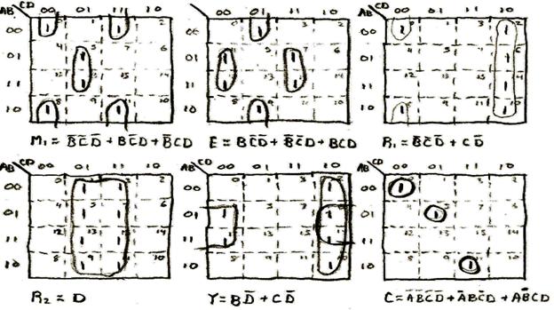
Despite the pattern looking somewhat symmetrical, each letter required its own decoding logic expect for the letters R1 and S1. These letters remain on throughout the entire sequence and as a result decode to logic 1.
M1 = B AND C AND NOT(D);
E = (B AND D) or (B AND C);
R1 = '1';
R2 = (NOT(B) AND D) or (NOT(B) AND C);
Y = NOT(B) AND C AND NOT(D);
C = A AND B AND NOT(C) AND NOT(D);
H = (A AND B AND NOT(C)) or (A AND NOT(B) AND C AND D);
R3 = (A AND B AND NOT(C)) or (A AND NOT(B) AND C) or (A AND C AND NOT(D));
I = (A AND B AND NOT(C)) or (A AND D) or (A AND C);
S1 = '1';
T = (NOT(A) AND B AND NOT(C)) or (NOT(A) AND D) or (NOT(A) AND C);
M2 = (NOT(A) AND B AND NOT(C)) or (NOT(A) AND NOT(B) AND C) or (NOT(A) AND C AND NOT(D));
A = (NOT(A) AND B AND NOT(C)) or (NOT(A) AND NOT(B) AND C AND D);
S2 = NOT(A) AND B AND NOT(C) AND NOT(D);
Sequence 7: Reverse Spin Sequence
The reverse spin sequence is simply the inversion of the spin sequence as shown in the truth table.
|
A |
B |
C |
D |
M |
E |
R |
R |
Y |
C |
H |
R |
I |
S |
T |
M |
A |
S |
|
0 |
0 |
0 |
0 |
1 |
1 |
||||||||||||
|
0 |
0 |
0 |
1 |
1 |
1 |
1 |
1 |
||||||||||
|
0 |
0 |
1 |
0 |
1 |
1 |
1 |
1 |
1 |
1 |
||||||||
|
0 |
0 |
1 |
1 |
1 |
1 |
1 |
1 |
1 |
1 |
||||||||
|
0 |
1 |
0 |
0 |
1 |
1 |
1 |
1 |
1 |
1 |
||||||||
|
0 |
1 |
0 |
1 |
1 |
1 |
1 |
1 |
1 |
1 |
||||||||
|
0 |
1 |
1 |
0 |
1 |
1 |
1 |
1 |
1 |
1 |
||||||||
|
0 |
1 |
1 |
1 |
1 |
1 |
1 |
1 |
||||||||||
|
1 |
0 |
0 |
0 |
1 |
1 |
||||||||||||
|
1 |
0 |
0 |
1 |
1 |
1 |
1 |
1 |
||||||||||
|
1 |
0 |
1 |
0 |
1 |
1 |
1 |
1 |
1 |
1 |
||||||||
|
1 |
0 |
1 |
1 |
1 |
1 |
1 |
1 |
1 |
1 |
||||||||
|
1 |
1 |
0 |
0 |
1 |
1 |
1 |
1 |
1 |
1 |
||||||||
|
1 |
1 |
0 |
1 |
1 |
1 |
1 |
1 |
1 |
1 |
||||||||
|
1 |
1 |
1 |
0 |
1 |
1 |
1 |
1 |
1 |
1 |
||||||||
|
1 |
1 |
1 |
1 |
1 |
1 |
1 |
1 |
Truth Table of the Reverse Spin Sequence
Just like the spin sequence, the reverse spin sequence requires each letter to have its own decoding logic with the letters R1 and S1 remaining on throughout the entire sequence.
M1 = NOT(B) AND C AND NOT(D);
E = (NOT(B) AND D) OR (NOT(B) AND C);
R1 = '1';
R2 = (B AND D) OR (B AND C);
Y = B AND C AND NOT(D);
C = NOT(A) AND B AND NOT(C) AND NOT(D);
H = (NOT(A) AND B AND NOT(C)) OR (NOT(A) AND NOT(B) AND C AND D);
R3 = (NOT(A) AND B AND NOT(C)) OR (NOT(A) AND NOT(B) AND C) OR (NOT(A) AND C AND NOT(D));
I = (NOT(A) AND B AND NOT(C)) OR (NOT(A) AND D) OR (NOT(A) AND C);
S1 = '1';
T = (A AND B AND NOT(C)) OR (A AND D) OR (A AND C);
M2 = (A AND B AND NOT(C)) OR (A AND NOT(B) AND C) OR (A AND C AND NOT(D));
A = (A AND B AND NOT(C)) OR (A AND NOT(B) AND C AND D);
S2 = A AND B AND NOT(C) AND NOT(D);
Sequence 8: Spread Sequence
The spread sequence was so named because the pattern appears to spread in and out down the truth table.
|
A |
B |
C |
D |
M |
E |
R |
R |
Y |
C |
H |
R |
I |
S |
T |
M |
A |
S |
|
0 |
0 |
0 |
0 |
1 |
1 |
||||||||||||
|
0 |
0 |
0 |
1 |
1 |
1 |
1 |
1 |
1 |
1 |
||||||||
|
0 |
0 |
1 |
0 |
1 |
1 |
1 |
1 |
1 |
1 |
1 |
1 |
1 |
1 |
||||
|
0 |
0 |
1 |
1 |
1 |
1 |
1 |
1 |
1 |
1 |
1 |
1 |
1 |
1 |
||||
|
0 |
1 |
0 |
0 |
1 |
1 |
1 |
1 |
1 |
1 |
1 |
1 |
1 |
1 |
||||
|
0 |
1 |
0 |
1 |
1 |
1 |
1 |
1 |
1 |
1 |
1 |
1 |
1 |
1 |
||||
|
0 |
1 |
1 |
0 |
1 |
1 |
1 |
1 |
1 |
1 |
1 |
1 |
1 |
1 |
||||
|
0 |
1 |
1 |
1 |
1 |
1 |
1 |
1 |
1 |
|||||||||
|
1 |
0 |
0 |
0 |
1 |
1 |
||||||||||||
|
1 |
0 |
0 |
1 |
1 |
1 |
1 |
1 |
1 |
1 |
||||||||
|
1 |
0 |
1 |
0 |
1 |
1 |
1 |
1 |
1 |
1 |
1 |
1 |
1 |
1 |
||||
|
1 |
0 |
1 |
1 |
1 |
1 |
1 |
1 |
1 |
1 |
1 |
1 |
1 |
1 |
||||
|
1 |
1 |
0 |
0 |
1 |
1 |
1 |
1 |
1 |
1 |
1 |
1 |
1 |
1 |
||||
|
1 |
1 |
0 |
1 |
1 |
1 |
1 |
1 |
1 |
1 |
1 |
1 |
1 |
1 |
||||
|
1 |
1 |
1 |
0 |
1 |
1 |
1 |
1 |
1 |
1 |
1 |
1 |
1 |
1 |
||||
|
1 |
1 |
1 |
1 |
1 |
1 |
1 |
1 |
1 |
1 |
Truth Table of the Spread Sequence
Like the spin sequences, the first letter R and the first letter S are on throughout the entire sequence. The truth table is decoded for each of the letters as follows.
M1, Y = C AND NOT(D);
E, R2 = D OR C;
R1 = '1';
C, S2 = B AND NOT(C) AND NOT(D);
H, A = (B AND NOT(C)) OR (NOT(B) AND C AND D);
R3, M2 = (B AND NOT(C)) OR (C AND NOT(D)) OR (NOT(B) AND C);
I, T = B OR D OR C;
S1 = '1';
Top-Level Component
The top-level component is implemented using the structural architecture in VHDL that maps the ports of the previous components together in the overall design.
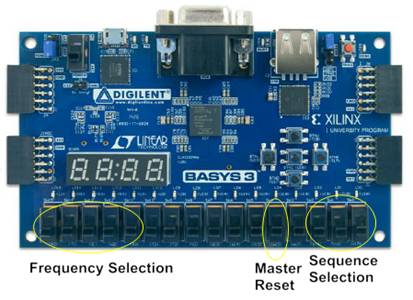
Figure 7: Input Constraints of the Top-Level Design
The constraints for the top-level component maps the sequence inputs to the far right three switches (V17, V16, and W16) of the Basys 3 trainer board. These switches select the one of the 8 sequences for the lights of this design. The five inputs used to select the frequency of the output signal of the frequency divider are mapped to the five switches on the far-left side of the Basys 3 trainer board. The master reset input is mapped to the fifth switch from the right (W15) on the trainer board.
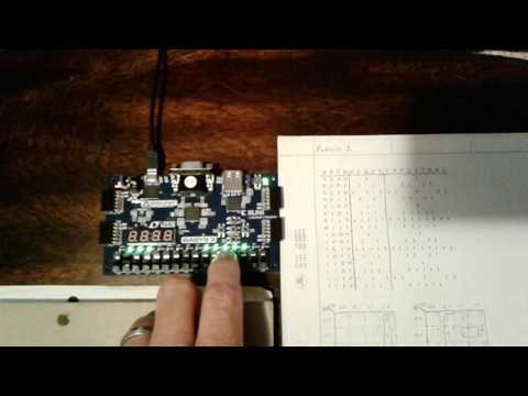
Figure 8: Video Presentation of the Final Design on the Basys 3
The Logic Probes
The final piece of the design is the logic probes that will light red on logic level high and green on logic level low. The design of the logic probes considered a five-volt logic signal since they were originally designed with TTL gates in mind. Since the Artix-7 FPGA device is a 3.3-volt logic device, level shifters will be needed to drive these probes with the Basys 3 trainer board. Originally, the logic probes were built using bipolar junction transistors but part way through the project I changed the design to utilize MOSFET transistors due to their much higher input impedances. The higher the input impedance, the more inputs that can be driven with a single output if any device.
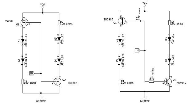
Figure 9: Logic Probe Schematics
The schematic on the left uses MOSFET and the one on the right uses BJTs.
My attempt to attach the logic probes to the Basys 3 device was only moderately successful. One probe functioned properly but the remaining probes held steady. The probes work so the issue must be between the Basys 3 device and the probes. Perhaps with the level shifters or perhaps the incorrect ports on the Basys 3 device were used.
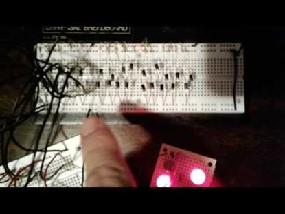
Figure 10: Final Design with Probes Attached
Schedule
The final schedule for the project shows that some parts of the project did come in late but the time frame gave me plenty of time to make up for most of it. Issues that were encountered which made some parts of the project design unavailable will be covered in later sections. The synthesizing, simulating, and testing of the design went along fairly smooth and was completed on time. Building of the logic probes came late due to lack of parts and the assembly of the final design was affected by it. The schedule was realistic given the design but unforeseen circumstances made parts of it late. Better planning and allowing extra time for “incidentals” would help to better deal with such situations on future projects.
|
Task |
Estimated Time |
Estimated Date of Completion |
Status |
|
Synthesize, Simulate, and Test |
One Week |
April 1, 2017 |
Completed |
|
Build and Test Logic Probes |
Three Days |
(April 16, 2017) |
Completed |
|
Assemble and Test Final Design |
One Week |
(April 23, 2017) |
90% |
Problems Encountered
While much of the testing went smoothly, various issues were encountered during the testing and simulation phases of the project design. Some of the issues involved bugs in the VHDL code where as others were due to simulations not going as expected even though the components functioned properly after being programmed in the FPGA device.
Frequency Divider Issues
The frequency divider component at first did not oscillate its output signal at all and I noticed this when I had already integrated it into a complete design for testing. The problem manifested itself on the Basys 3 trainer board by lighting the pattern on the first interval for the sequences based on the sequence selected. Changing the sequence changed the light pattern but the sequence never progressed. After deeper investigation, I determined that the source of the problem was with the frequency divider and managed to isolate it to the VHDL that used the frequency selection to determine the frequency of its output signal.
|
-- The frequency divider output stage. FRQDIV: process(CLK_HZ, CLK_SEL) variable count : std_logic_vector(4 downto 0); variable outp : std_logic := '0'; begin -- Increment count on rising edge of CLK_HZ. if CLK_HZ'event and CLK_HZ = '1' then count := count + 1; -- Setup the output clock
port. for i in 4 downto 0 loop outp := outp or (CLK_SEL(i) and count(i)); end loop; end if; -- Set the output clock signal. CLK_OUT <= outp; end process; |
|
VHDL
Listing with the offending lines highlighted. |
From a software perspective, the process would appear to work properly but
since I was unable to get a good simulation using either the Active HDL or the
Xilinx Vivado software I was unable to determine exactly which line was causing
the output signal to fail to oscillate. The
resolution was to simply replace the highlight code with a simpler
implementation which solved the problem.
|
-- The frequency divider output stage. FRQDIV: process(CLK_HZ, CLK_SEL) variable count : std_logic_vector(4 downto 0); variable outp : std_logic_vector(4 downto 0); begin -- Increment count on rising edge of CLK_HZ. if CLK_HZ'event and CLK_HZ = '1' then count := count + 1; -- Setup the output clock
port. for i in 4 downto 0 loop outp(i) := (CLK_SEL(i) and count(i)); end loop; end if; -- Set the output clock signal. CLK_OUT <= outp(4) or outp(3) or outp(2) or outp(1) or outp(0); end process; |
|
VHDL
Listing of the corrected process. |
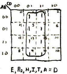
Decoder Issues
The only issue encountered with the decoder stage was with the double zig zag sequence (sequence number 5). The first letter M (that begins the word Merry) was not following the pattern in the truth table for this sequence. It was difficult to keep track of which intervals (0 to 15) the LED for this letter was on when it was supposed to be off when testing on the Basys 3 device so a simulation was performed to generate a wave form of the sequence.
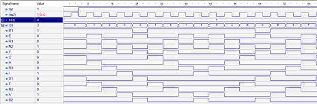
Figure 11: Waveform for Double Zig Zag Sequence
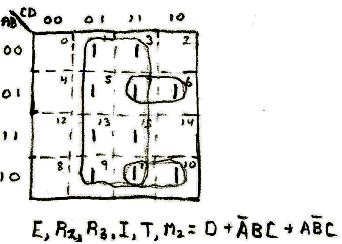
Looking at the waveform generated, I can see that the first letter M was only off (low) for intervals 4 and 12. This, of course, did not agree with the truth table where the letter was supposed to be on only for intervals 0, 3, 5, 8, 11, and 13. I double checked the K-Map to make sure I did not get the wrong decoding logic based on the truth table but everything checked out okay on the K-Map.
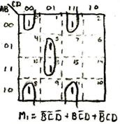
Figure 12: K-Map Decoding for M1
After examining the VHDL for this letter for this sequence, I discovered where the last part of the equation (NOT(B) AND C AND D) was coded incorrectly.
|
when "100" => -- Double Zig Zag Sequence M1 <= (nQb and nQc and nQd) or (Qb and nQc and Qd) or (nQb or Qc or Qd); |
|
VHDL
snippet with the erroneous code highlighted |
Replacing the OR’s with AND’s corrected the problem and another waveform
simulation was generated to verify that this sequence had been corrected.
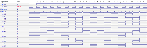
Figure 13: Corrected Waveform for Double Zig Zag Sequence
The corrected waveform now properly shows that the letter M1 is high only for the correct intervals.
Hardware Issues
These weren’t so much issues with the additional hardware but more of availability of the parts needed to fully build and test the design. In searching for similar LEDs for the logic probes that I used with the bipolar junction transistor probes that I built years ago for the old design, I had a difficult time locating the LEDs. I was, on the other hand, fortunate to manage to get to a Radio Shack and buy their remaining stock of protoboards that I used to build a prototype of the probes before they shut their doors for good. One such Radio Shack where I live is privately owned and has become a father and son electronics shop called Gizmos. I managed get some high bright red LEDs from these stores but not any green ones. The son at the Gizmos store offered to order some for me but I turned him down at the time to see if I could find them elsewhere first. After a few days of no success, I called the store back to inquire about ordering the parts only to find I was too late and that another order would not take place until April 10th.
Fortune, however, glanced my way when I started looking around in the attic for any additional parts and found bags of LEDs I had ordered from Jameco just for old project. I was delighted to see that the bags even had the part numbers and that Jameco still carried the parts, so I ordered them online and got them in a few days. Along with the LEDs, I also ordered the transistors and resistors to complete the probes. However, despite my good fortune, I still managed to come up one logic probe short due to a lack of green LEDs, (I was two LEDs short) and with the deadline looming I decided to try one of probes that uses the BJTs instead of the MOSFETs. They work in a five-volt logic system but don’t work properly with 3.3 volts with the level shifting circuit that I employed.
Level shifting was the other surprise I had encountered during the testing phase. I had built the probes based on the schematics I had laid out but these schematics were designed with a 5-volt logic system in mind. When I discovered that the Artix-7 is a 3.3-volt device, I panicked and scrambled for an inexpensive and easy to implement level shifting circuit design that I could use to test the probes with the Basys 3 device. I managed to find a simple circuit design that only requires two diodes and a resistor but I did not have enough diodes or 10K-ohm resistors on hand to build 14 level shifters. I search online at Digikey for the components and I found them very cheap but the cost of shipping would exceed the cost of the parts. Therefore, I tried the Radio Shack again and found that it was still open even though most of their shelves were empty. They also sold their components for 90% off which was very fortunate indeed as I bought 50 of their diodes and 15 of their 10k-ohm resistors.
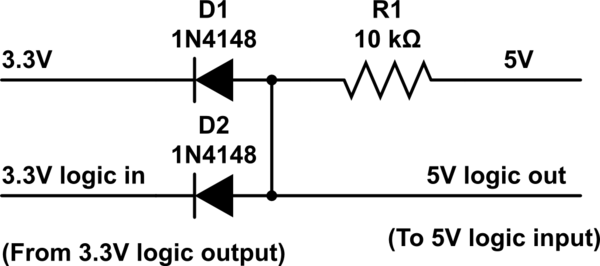
Figure 14: Level Shifters for the Probes
Finally, there was the UM66 IC hardware that I mentioned early on that generates the music for this project. I was not so fortunate to find this device to add to this project. Granted, this part of the project was not promised but was mentioned as I did originally want to include some music to go along with the lights. Considering that, I searched Digikey and Mouser and was unable to find the part. Then I did a broader search on Google only to find some E-Bay vendors that no longer had the part. I did come across one forum that mentioned that this device was obsolete and suggested some alternatives but I was unable to even find them at Digikey or Mouser. At best, I might have been able to order them from a vendor in China but the shipping time of about a month or so would mean that they would not arrive in time given the time frame for this project.
Future Work
During the design and testing of this project I thought of what else was out there that I could use the Artix-7 FPGA device to do. One idea I had was to take this to the next level and add music where I could synchronize the lights to. On a grander level, the output logic could be used to drive solid state relays and have the lights in the yard light in a predetermined sequence or to synchronize to music. Regarding what I would do different with this project, I wish I had more time to rework the logic probes and build the support circuitry to make these probes work with both 3.3 and 5-volt logic. It would not be too complicated to accomplish but time was running out and I had to make do with what I had.
Conclusion
This project was both challenging and rewarding to build and test. With it, I learned about customizing the Clocking Wizard IP to generate a custom frequency for my design and learned a bit about the nuances of VHDL and how it behaves differently from conventional programming languages while I was attempting to correct the issues with the frequency divider component. Building the binary counter and seeing it in action was a delight but the watching the whole design come alive with the addition of the decoder and the top-level components was certainly something to see. I must confess, I never actually finished the original design that utilized a 555 timer, an actual 74161 binary counter, and the 7400 TTL logic for the decoding but I kept the designs for this around as I had always intended to get around to building it.
Building more “complicated” sequences would be a non-starter if TTL logic chips were employed and I had always considered the possibility of using programmable logic chips for some of the more complicated decoding sequences. Thanks to the capabilities of the Artix-7 FPGA device, I could accomplish the more complicated sequences and add even more functionality than I had originally thought possible. Functions such as adjusting the sequences and the frequencies is something that would be next to impossible to do with TTL logic chips (at least without requiring a large amount of them). While these functions could very simply be written in an embedded software application for a microcontroller, this method just seems like a tad bit of overkill. The FPGA device provided the right balance for designing more sophisticated logic devices without requiring the overhead of a microcontroller or the high expense of an ASIC.
References
FAST and LS TTL data.
(1992). Phoenix, AZ: Motorola.
Basys 3 FPGA Reference Manual. (n.d.). Digilent.
Skahill, K. (1998). VHDL
for programmable logic. Reading, MA: Addison-Wesley Longman Higher
Education.
Donald, F. D. (2015, April 17). Musical Greeting Card circuit using UM66 IC. Retrieved February 12, 2017, from http://www.gadgetronicx.com/musical-greeting-card-um66ic/
Appendix
The implementation of the design (VHDL, K-Maps) can be found in this section.
Frequency Divider VHDL Listing
The frequency divider component is implemented using the behavioral architecture utilizing two processes. The first process divides the 16 MHz signal to 16 Hz and the second stage divides the 16 Hz signal to one of five selectable frequencies of 1, 2, 4, 8, and 16 Hz.
library IEEE;
use IEEE.STD_LOGIC_1164.ALL;
use IEEE.STD_LOGIC_UNSIGNED.all;
entity FreqDiv is
Port ( CLK_SEL : in STD_LOGIC_VECTOR (4 downto 0); -- Clock selection.
CLK_IN : in STD_LOGIC;
CLK_OUT : out STD_LOGIC);
end FreqDiv;
architecture Behavioral of FreqDiv is
signal CLK_HZ : std_logic;
begin
--
The MHz to Hz stage of the frequency divider.
MHz2Hz: process(CLK_IN)
variable mhertz_count : std_logic_vector(19 downto 0);
begin
--
Increment the count on the rising edge of the clock.
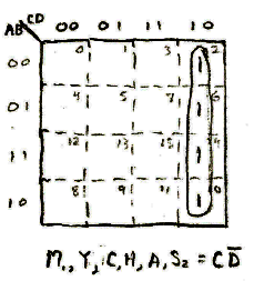
if CLK_IN'event and CLK_IN = '1' then
mhertz_count := mhertz_count + 1;
end if;
--
Set the clock in Hz signal to MSB of count.
CLK_HZ <= mhertz_count(19);
end process;
--
The frequency divider output stage.
FRQDIV: process(CLK_HZ, CLK_SEL)
variable count : std_logic_vector(4 downto 0);
variable outp : std_logic_vector(4 downto 0);
begin
--
Increment count on rising edge of CLK_HZ.
if CLK_HZ'event and CLK_HZ = '1' then
count := count + 1;
--
Setup the output clock port.
for i in 4 downto 0 loop
outp(i) := (CLK_SEL(i) and count(i));
end loop;
end if;
--
Set the output clock signal.
CLK_OUT <= outp(4) or outp(3) or outp(2) or outp(1) or outp(0);
end process;
end Behavioral;
Binary Counter VHDL Listing
The VHDL listing for the binary counter emulates in VHDL the functions of the 74161 binary counter chip as described in the Fast and LS TTL Data book published by Motorola in 1992. This component is implemented using the behavioral architecture in VHDL.
library IEEE;
use IEEE.STD_LOGIC_1164.ALL;
use IEEE.STD_LOGIC_UNSIGNED.all;
-- Entity declaration of
the MC74161A device.
entity MC74161A is
Port ( MR : in STD_LOGIC; --
Master Reset (active low)
CLK : in STD_LOGIC; -- Clock (increments on rising edge)
PE : in STD_LOGIC; -- Parallel enable (loads Q with P on CLK)
CET : in STD_LOGIC; -- Clock enable trickle.
CEP : in STD_LOGIC; -- Count enable parallel.
P : in STD_LOGIC_VECTOR (3 downto 0); --
Parallel input
TC : out STD_LOGIC; -- Terminal Count
Q : out STD_LOGIC_VECTOR (3 downto 0)); -- Q output.
end MC74161A;
-- Behavioral architecture
of the MC74161A device.
architecture Behavioral of MC74161A is
begin
process(MR, CLK)
variable Qout : std_logic_vector(3 downto 0);
begin
--
Check sensitivity list.
if (MR = '0') then
--
Asynchronous Master Reset.
Qout := "0000";
elsif (CLK'event and CLK = '1') then
--
Perform other operations on rising edge of clock.
if (PE = '0') then
-- Parallel Enable (aka Parallel Load) loads P.
Qout := P;
elsif (CET = '1' and CEP = '1') then
-- Count Enable Trickle
-- Count Enable Parallel
-- Both must be high to count.
Qout := Qout + 1;
end if;
end if;
--
Set the output signals (Q and TC).
Q <= Qout;
TC <= Qout(3) and Qout(2) and Qout(1) and Qout(0);
end process;
end Behavioral;
Decoder VHDL Listing
The decoder stage of the design takes the Q outputs of the binary counter component and decodes them for each of the 14 letters that spell Merry Christmas according to the currently selected sequence. The overall architecture of this component is behavioral while the decoding logic itself is structural.
library IEEE;
use IEEE.STD_LOGIC_1164.ALL;
entity Decoder is
Port ( Qin : in std_logic_vector(3 downto 0); --
Output from counter.
SEQ : in STD_LOGIC_VECTOR(2 downto 0); -- Selected sequence.
M1, E, R1, R2, Y : out std_logic; -- Decoded outputs
C, H, R3, I, S1, T, M2, A, S2 : out std_logic); -- Decoded outputs
end Decoder;
architecture Behavioral of Decoder is
begin
--
Sensitive to changes in Qin and SEQ.
process(Qin, SEQ)
variable Qa, Qb, Qc, Qd, nQa, nQb, nQc, nQd : std_logic;
begin
--
Copy the Q input signals to the Qx variables.
Qa := Qin(3);
Qb := Qin(2);
Qc := Qin(1);
Qd := Qin(0);
--
Invert and copy the Q input signals to the nQx variables.
nQa := not Qin(3);
nQb := not Qin(2);
nQc := not Qin(1);
nQd := not Qin(0);
--
Determine which sequence is selected.
case SEQ is
when "000" => --
Original Design.
M1 <= Qc and nQd;
E <= Qd or (nQa and Qb and Qc) or (Qa and nQb and Qc);
R1 <= Qb or nQd;
R2 <= Qd or (nQa and Qb and Qc) or (Qa and nQb and Qc);
Y <= Qc and nQd;
C <= Qc and nQd;
H <= Qc and nQd;
R3 <= Qd or (nQa and Qb and Qc) or (Qa and nQb and Qc);
I <= Qd or (nQa and Qb and Qc) or (Qa and nQb and Qc);
S1 <= Qb or nQd;
T <= Qd or (nQa and Qb and Qc) or (Qa and nQb and Qc);
M2 <= Qd or (nQa and Qb and Qc) or (Qa and nQb and Qc);
A <= Qc and nQd;
S2 <= Qc and nQd;
when "001" => --
Simple Alternating Sequence
M1 <= nQd;
E <= Qd;
R1 <= nQd;
R2 <= Qd;
Y <= nQd;
C <= nQd;
H <= Qd;
R3 <= nQd;
I <= Qd;
S1 <= nQd;
T <= Qd;
M2 <= nQd;
A <= Qd;
S2 <= nQd;
when "010" => --
Zig Zag Sequence
M1 <= nQb and nQc and nQd;
E <= (nQb and nQc and Qd) or (Qb and Qc and Qd);
R1 <= Qc and nQd;
R2 <= (Qb and nQc and Qd) or (nQb and Qc and Qd);
Y <= Qb and nQc and nQd;
C <= nQa and nQb and nQc and nQd;
H <= (nQa and nQb and nQc and Qd) or (Qa and Qb and Qc and Qd);
R3 <= (nQa and nQb and Qc and nQd) or (Qa and Qb and Qc and nQd);
I <= (nQa and nQb and Qc and Qd) or (Qa and Qb and nQc and Qd);
S1 <= Qb and nQc and nQd;
T <= (nQa and Qb and nQc and Qd) or (Qa and nQb and Qc and Qd);
M2 <= (nQa and Qb and Qc and nQd) or (Qa and nQb and Qc and nQd);
A <= (nQa and Qb and Qc and Qd) or (Qa and nQb and nQc and Qd);
S2 <= Qa and nQb and nQc and nQd;
when "011" => --
Diamond Sequence
M1 <= Qc and nQd;
E <= Qd;
R1 <= nQc and nQd;
R2 <= Qd;
Y <= Qc and nQd;
C <= Qb and nQc and nQd;
H <= (Qb and nQc and Qd) or (nQb and Qc and Qd);
R3 <= Qc and nQd;
I <= (nQb and nQc and Qd) or (Qb and Qc and Qd);
S1 <= nQb and nQc and nQd;
T <= (nQb and nQc and Qd) or (Qb and Qc and Qd);
M2 <= Qc and nQd;
A <= (Qb and nQc and Qd) or (nQb and Qc and Qd);
S2 <= Qb and nQc and nQd;
when "100" => --
Double Zig Zag Sequence
M1 <= (nQb and nQc and nQd) or (Qb and nQc and Qd) or (nQb and Qc and Qd);
E <= (Qb and nQc and nQd) or (nQb and nQc and Qd) or (Qb and Qc and Qd);
R1 <= (nQb and nQc and nQd) or (Qc and nQd);
R2 <= Qd;
Y <= (Qb and nQd) or (Qc and nQd);
C <= (nQa and nQb and nQc and nQd) or
(nQa and Qb and nQc and Qd) or
(Qa and nQb and Qc and Qd);
H <= (nQa and nQb and nQc and Qd) or
(nQa and Qb and Qc and nQd) or
(Qa and nQb and Qc and nQd) or
(Qa and Qb and Qc and Qd);
R3 <= (nQa and nQb and Qc and nQd) or
(nQa and Qb and Qc and Qd) or
(Qa and nQb and nQc and Qd) or
(Qa and Qb and Qc and nQd);
I <= (nQa and nQb and Qc and Qd) or (Qa and nQb and nQc and nQd) or
(Qa and Qb and nQc and Qd);
S1 <= (nQa and nQc and nQd) or (Qb and nQc and nQd);
T <= (nQa and nQc and Qd) or (Qa and Qc and Qd);
M2 <= Qc and nQd;
A <= (nQa and Qc and Qd) or (Qa and nQc and Qd);
S2 <= (Qb and nQc and nQd) or (Qa and nQc and nQd);
when "101" => --
Spin Sequence
M1 <= Qb and Qc and nQd;
E <= (Qb and Qd) or (Qb and Qc);
R1 <= '1';
R2 <= (nQb and Qd) or (nQb and Qc);
Y <= nQb and Qc and nQd;
C <= Qa and Qb and nQc and nQd;
H <= (Qa and Qb and nQc) or (Qa and nQb and Qc and Qd);
R3 <= (Qa and Qb and nQc) or (Qa and nQb and Qc) or (Qa and Qc and nQd);
I <= (Qa and Qb and nQc) or (Qa and Qd) or (Qa and Qc);
S1 <= '1';
T <= (nQa and Qb and nQc) or (nQa and Qd) or (nQa and Qc);
M2 <= (nQa and Qb and nQc) or (nQa and nQb and Qc) or (nQa and Qc and nQd);
A <= (nQa and Qb and nQc) or (nQa and nQb and Qc and Qd);
S2 <= nQa and Qb and nQc and nQd;
when "110" => --
Reverse Spin Sequence
M1 <= nQb and Qc and nQd;
E <= (nQb and Qd) or (nQb and Qc);
R1 <= '1';
R2 <= (Qb and Qd) or (Qb and Qc);
Y <= Qb and Qc and nQd;
C <= nQa and Qb and nQc and nQd;
H <= (nQa and Qb and nQc) or (nQa and nQb and Qc and Qd);
R3 <= (nQa and Qb and nQc) or (nQa and nQb and Qc) or (nQa and Qc and nQd);
I <= (nQa and Qb and nQc) or (nQa and Qd) or (nQa and Qc);
S1 <= '1';
T <= (Qa and Qb and nQc) or (Qa and Qd) or (Qa and Qc);
M2 <= (Qa and Qb and nQc) or (Qa and nQb and Qc) or (Qa and Qc and nQd);
A <= (Qa and Qb and nQc) or (Qa and nQb and Qc and Qd);
S2 <= Qa and Qb and nQc and nQd;
when "111" => --
Spread Sequence
M1 <= Qc and nQd;
E <= Qd or Qc;
R1 <= '1';
R2 <= Qd or Qc;
Y <= Qc and nQd;
C <= Qb and nQc and nQd;
H <= (Qb and nQc) or (nQb and Qc and Qd);
R3 <= (Qb and nQc) or (Qc and nQd) or (nQb and Qc);
I <= Qb or Qd or Qc;
S1 <= '1';
T <= Qb or Qd or Qc;
M2 <= (Qb and nQc) or (Qc and nQd) or (nQb and Qc);
A <= (Qb and nQc) or (nQb and Qc and Qd);
S2 <= Qb and nQc and nQd;
when others =>
M1 <= 'Z';
E <= 'Z';
R1 <= 'Z';
R2 <= 'Z';
Y <= 'Z';
C <= 'Z';
H <= 'Z';
R3 <= 'Z';
I <= 'Z';
S1 <= 'Z';
T <= 'Z';
M2 <= 'Z';
A <= 'Z';
S2 <= 'Z';
end case;
end process;
end Behavioral;
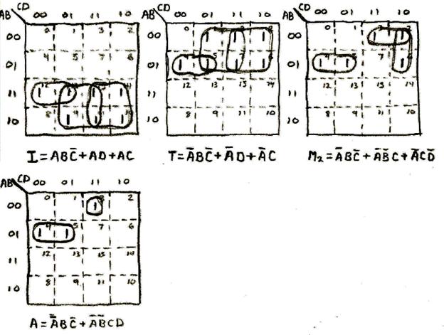
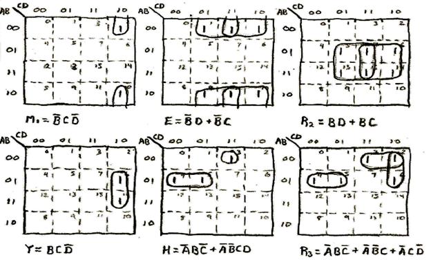
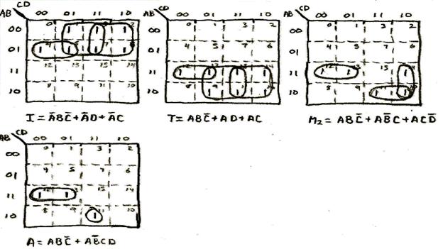
Decoder Stage Karnaugh Maps
The karnaugh maps (K-Maps) used to determine the decoding logic for each sequence are provided in the following sections.
Sequence 1: Original Design Sequence
Three K-Maps was all it took to fully decode this sequence.
Sequence 2: Simple Alternating Sequence
This sequence was so simple that the K-Maps were not even required to decode it. The use of the K-Maps does confirm that the entire sequence can be decoded by simply taking the least significant bit of the output signal Q on the counter (signal D in the decoder) into account.
Sequence 3: Zig Zag Sequence
This sequence is one of the two most complicated (from a decoding logic standpoint) sequences in the design.
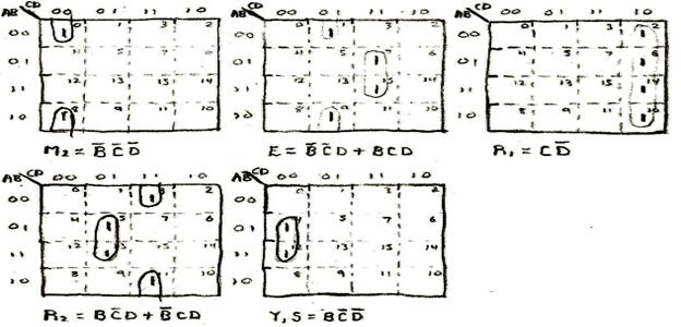
Sequence 4: Diamond Sequence
This sequence has more symmetry as well as more overlap. That is, multiple letters followed the same sequence individually throughout this overall pattern.
Sequence 5: Double Zig Zag Sequence
This sequence is the most complicated (from a decoding perspective) of all the sequences in this design.
Sequence 6: Spin Sequence
This sequence always has the first letter R and the first letter S set to logic 1 throughout. As such, no K-Map was required to decode these letters since the letters will simply reduce to being decoded as logic 1. In addition to no K-Maps being provided for these two letters, no K-Maps were required for the first and last letters (C and S) of Christmas since they only turn on once throughout the entire sequence and therefore decode to the A, B, C, and D signals for those intervals.
C = A AND B AND NOT(C) AND NOT(D)
S2 = NOT(A) AND B AND NOT(C) AND NOT(D)
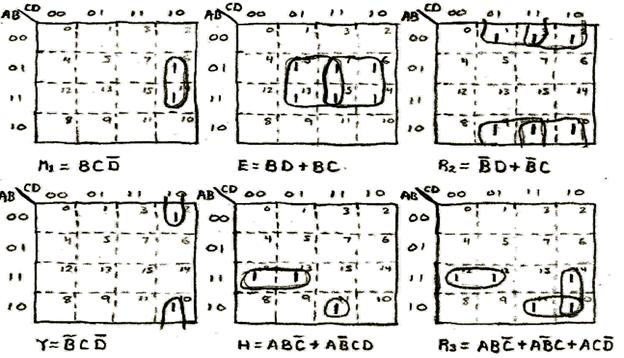
Sequence 7: Reverse Spin Sequence
This sequence is basically the mirror opposite of the spin sequence. Like the spin sequence, the first letter R and the first letter S are always on and therefore no K-Map was required to decode. Also, the first and last letters of Christmas was also not decoded using K-Maps since they come on only once throughout the sequence.
C = NOT(A) AND B AND NOT(C) AND NOT(D)
S2 = A AND B AND NOT(C) AND NOT(D)
Sequence 8: Spread Sequence
The last sequence of this design. Like the spin sequences, the spread sequence also decodes the first letter R and the first letter S as logic 1.
Top-Level Component VHDL Listing
The top-level component uses the structural architecture and binds the components together to generate the final design.
library IEEE;
use IEEE.STD_LOGIC_1164.ALL;
entity top_level is
Port ( mclk : in STD_LOGIC;
frq : in std_logic_vector(4 downto 0);
seqn : in std_logic_vector(2 downto 0);
mr : in std_logic;
Lm1, Le, Lr1, Lr2, Ly : out std_logic;
Lc, Lh, Lr3, Li, Ls1, Lt, Lm2, La, Ls2 : out std_logic);
end top_level;
architecture Structural of top_level is
component pri_clk
port
(-- Clock in ports
--
Clock out ports
pclk : out std_logic;
--
Status and control signals
resetn : in std_logic;
locked : out std_logic;
mclk : in std_logic
);
end component;
component FreqDiv
Port ( CLK_SEL : in STD_LOGIC_VECTOR (4 downto 0); -- Clock selection.
CLK_IN : in STD_LOGIC;
CLK_OUT : out STD_LOGIC);
end component;
component MC74161A
Port ( MR : in STD_LOGIC; --
Master Reset (active low)
CLK : in STD_LOGIC; -- Clock (increments on rising edge)
PE : in STD_LOGIC; -- Parallel enable (loads Q with P on CLK)
CET : in STD_LOGIC; -- Clock enable trickle.
CEP : in STD_LOGIC; -- Count enable parallel.
P : in STD_LOGIC_VECTOR (3 downto 0); --
Parallel input
TC : out STD_LOGIC; -- Terminal Count
Q : out STD_LOGIC_VECTOR (3 downto 0)); -- Q output.
end component;
component Decoder is
Port ( Qin : in std_logic_vector(3 downto 0); --
Output from counter.
SEQ : in STD_LOGIC_VECTOR(2 downto 0); -- Selected sequence.
M1, E, R1, R2, Y : out std_logic; -- Decoded outputs
C, H, R3, I, S1, T, M2, A, S2 : out std_logic); -- Decoded outputs
end component;
signal clkp : std_logic;
signal clk_ctr : std_logic;
signal Qs : std_logic_vector(3 downto 0);
signal mr_n : std_logic;
begin
U0: pri_clk port map (mclk => mclk, resetn => mr, pclk => clkp);
U1: FreqDiv port map (CLK_SEL => frq, CLK_IN => clkp, CLK_OUT => clk_ctr);
U2: MC74161A port map (MR => mr, CLK => clk_ctr, PE => '1', CET => '1', CEP => '1', P => "0000", Q => Qs);
U3: Decoder port map (Qin => Qs,
SEQ => seqn,
M1 => Lm1, E => Le, R1 => Lr1, R2 => Lr2, Y => Ly,
C => Lc, H => Lh, R3 => Lr3, I => Li, S1 => Ls1, T => Lt, M2 => Lm2, A => La, S2 => Ls2);
end Structural;
Top-Level Constraints
The top-level constraints listing is provided to build this project into the Basys 3 trainer board that utilizes the Artix-7 FPGA device.
## Clock signal
set_property PACKAGE_PIN
W5 [get_ports mclk]
set_property IOSTANDARD LVCMOS33 [get_ports
mclk]
## Switches
set_property PACKAGE_PIN
V17 [get_ports {seqn[0]}]
set_property IOSTANDARD LVCMOS33 [get_ports
{seqn[0]}]
set_property PACKAGE_PIN
V16 [get_ports {seqn[1]}]
set_property IOSTANDARD LVCMOS33 [get_ports
{seqn[1]}]
set_property PACKAGE_PIN
W16 [get_ports {seqn[2]}]
set_property IOSTANDARD LVCMOS33 [get_ports
{seqn[2]}]
set_property PACKAGE_PIN
W15 [get_ports {mr}]
set_property IOSTANDARD LVCMOS33 [get_ports
{mr}]
set_property PACKAGE_PIN
R3 [get_ports {frq[0]}]
set_property IOSTANDARD LVCMOS33 [get_ports
{frq[0]}]
set_property PACKAGE_PIN
W2 [get_ports {frq[1]}]
set_property IOSTANDARD LVCMOS33 [get_ports
{frq[1]}]
set_property PACKAGE_PIN
U1 [get_ports {frq[2]}]
set_property IOSTANDARD LVCMOS33 [get_ports
{frq[2]}]
set_property PACKAGE_PIN
T1 [get_ports {frq[3]}]
set_property IOSTANDARD LVCMOS33 [get_ports
{frq[3]}]
set_property PACKAGE_PIN
R2 [get_ports {frq[4]}]
set_property IOSTANDARD LVCMOS33 [get_ports
{frq[4]}]
## LEDs
set_property PACKAGE_PIN
U16 [get_ports {Ls2}]
set_property IOSTANDARD LVCMOS33 [get_ports
{Ls2}]
set_property PACKAGE_PIN
E19 [get_ports {La}]
set_property IOSTANDARD LVCMOS33 [get_ports
{La}]
set_property PACKAGE_PIN
U19 [get_ports {Lm2}]
set_property IOSTANDARD LVCMOS33 [get_ports
{Lm2}]
set_property PACKAGE_PIN
V19 [get_ports {Lt}]
set_property IOSTANDARD LVCMOS33 [get_ports
{Lt}]
set_property PACKAGE_PIN
W18 [get_ports {Ls1}]
set_property IOSTANDARD LVCMOS33 [get_ports
{Ls1}]
set_property PACKAGE_PIN
U15 [get_ports {Li}]
set_property IOSTANDARD LVCMOS33 [get_ports
{Li}]
set_property PACKAGE_PIN
U14 [get_ports {Lr3}]
set_property IOSTANDARD LVCMOS33 [get_ports
{Lr3}]
set_property PACKAGE_PIN
V14 [get_ports {Lh}]
set_property IOSTANDARD LVCMOS33 [get_ports
{Lh}]
set_property PACKAGE_PIN
V13 [get_ports {Lc}]
set_property IOSTANDARD LVCMOS33 [get_ports
{Lc}]
set_property PACKAGE_PIN
U3 [get_ports {Ly}]
set_property IOSTANDARD LVCMOS33 [get_ports
{Ly}]
set_property PACKAGE_PIN
P3 [get_ports {Lr2}]
set_property IOSTANDARD LVCMOS33 [get_ports
{Lr2}]
set_property PACKAGE_PIN
N3 [get_ports {Lr1}]
set_property IOSTANDARD LVCMOS33 [get_ports
{Lr1}]
set_property PACKAGE_PIN
P1 [get_ports {Le}]
set_property IOSTANDARD LVCMOS33 [get_ports
{Le}]
set_property PACKAGE_PIN
L1 [get_ports {Lm1}]
set_property IOSTANDARD LVCMOS33 [get_ports
{Lm1}]